 产品列表 产品列表 |
|
|
|
|
|
|
 产
品 展 示 产
品 展 示 |
|
封装测试/PACKING TESTING >> 晶圆表面缺陷检测系统
|
|
 |
|
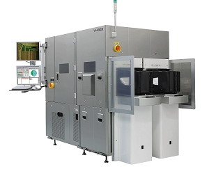
全自动晶圆表面缺陷检测设备 Wafer AOI

| |
Vi-4202R |
Vi-4304C |
| Camera |
4M Monochrome |
4M Color |
| Wafer Size |
~200mm |
~300mm |
| Handling |
Robot |
| Loader |
Open Cassette |
Open Cassette, FOUP, FOSB |
| Defect Size(μm) |
1.2/ 2.4 / 5.0 (objective lens 10x / 5x / 2.5x) |
| Size |
1600mm(W) x 1300mm(D) x 1800mm(H) |
2280mm(W) x 1140mm(D) x 2060mm(H) |
| Weight |
1200kg |
1700kg |
| Application |
CMOS image sensor, POWER device, RF filter, BUMP, MEMS |
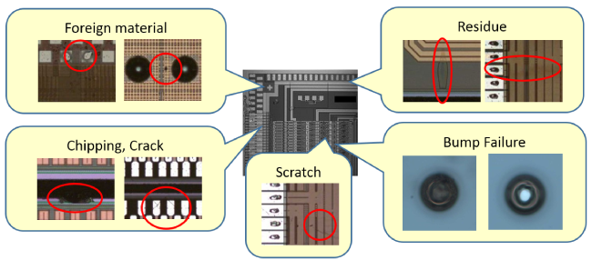
1. Example of defects

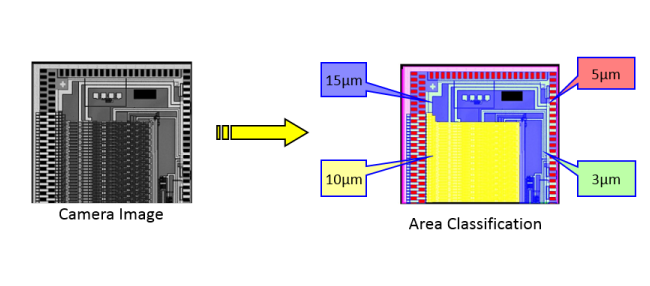
2. Fine detection by area(layer) classification
- The area classification realizes multiple inspection sensitivity and tolerance depending on features of device pattern.
- Each area can have inspection parameters.

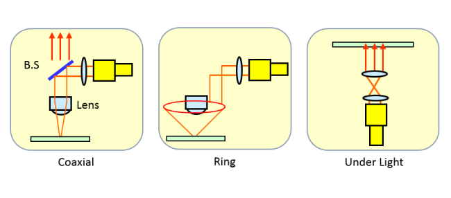
3. Refined image by various lighting and color image
- Defects that cannot be detected by grayscale inspection can be detected by color inspection.
- Combination of various light makes invisible defects see.

|
|
 |
| 点击数:1232 录入时间:2020/5/18 【打印此页】 【返回】 |
|
|
|
