|
Non-patterned 300mm Wafer surface Inspection system
无图形晶圆表面缺陷检测系统
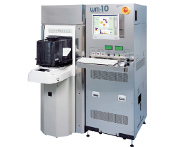
WM - 10 is a standard model of 300 mm wafer.
It is a high sensitivity inspection system of 48 nm.
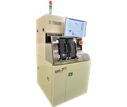
WM - 7 series is the most reasonable high - performance model below 200 mm wafer size.
WM - 7SG can inspect transparent wafers.
| |
WM-10 |
WM-7S/7SG |
| Sensitivity |
48nm@Bare-Wafer |
80nm@Bare-wafer:WM-7S
200nm@Glass-wafer:WM-7SG
|
| Wafer Size |
~300mm |
~200mm |
| Optical Source |
Laser Diode(405nm) |
| Loader |
FOUP(1 or2)/Open Cassette |
Open Cassette |
| Size |
1500mm×1300mm×1750mm |
860mm×900mm×1650mm |
| Application |
Bare-wafer/Filmed-wafer |
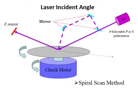
- WM-10 have 2axis Incident angle for particle.
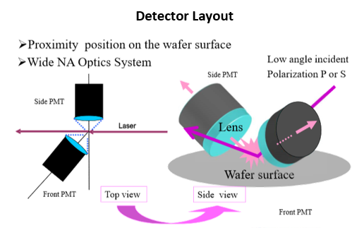
- WM-series have 2 wide NA lens for High-sensitivity detected.
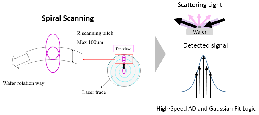
2. Spiral Scan With high-resolution XY-potsion
- WM-series are spiral scan method with rotation speed control.
- XY-Data send to EB review Equipment then it can be review with easy alignment.
|


 产品列表
产品列表